|

To do spreading resistance analysis one needs to identify a suitably large area containing the desired structure. The area needed, one of the smallest areas required
by any profiling technique, can usually be found on the chip, but this is often less than optimum. As a long term solution, dedicated spreading resistance test structures
are suggested. Sooner or later, a new test pattern will be laid out anyway and often these features can be included with negligible time and expense. The spreading resistance
test patterns offer the following advantages:
- complete characterization of the wafer fab process
- minimum analysis cost
- optimum resolution
- clear straight-forward identification of all possible doping structures
Every structure of possible interest can be produced by selectively exposing rectangles at the appropriate masking steps.
|
Structures of interest for a CMOS process might be:
- epi/substrate
- p-well/epi
- n-well/epi
- poly/gate ox/epi
- poly/gate ox/n-channel structure
- poly/gate ox/p-channel structure
- p+/epi
- p+/n-well
- n+/epi
- n+/p-well
- nldd
- pldd
- under field oxidation with implant
- under field oxidation without implant
|
Structures of interest for a "Classic" bipolar process might be:
- base/epi
- base/epi/buried layer/substrate
- base/isolation/epi/substrate
- emitter/base/epi
- emitter/base/epi/buried layer
- epi/buried layer/substrate
- epi/substrate
- extrinsic base/epi
- extrinsic base/epi/buried layer
- isolation/epi/substrate
- sinker/epi/buried layer
- sinker/epi/substrate
|
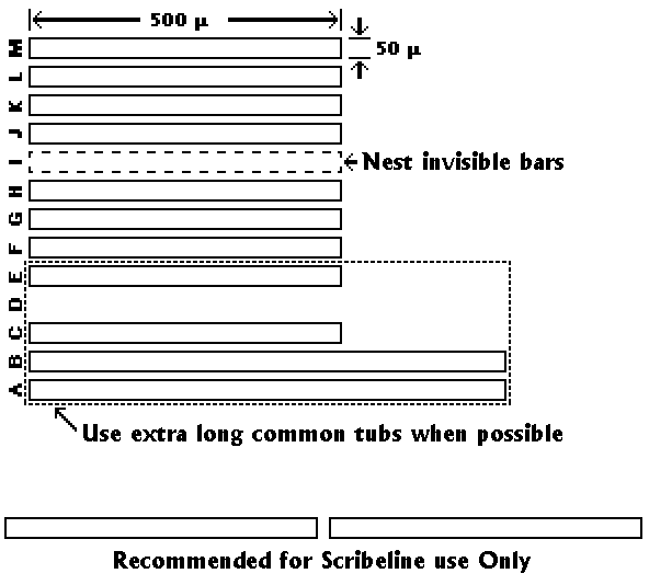
Illustration of Dedicated Spreading Resistance Test Patterns
|
NOTES
- If there is a very shallow emitter/base and a very deep buried layer a 100um x 1000um structure is suggested.
- In general, longer is always better-say up to 1500um.
- Width can be a problem as the number of patterns increases. please reduce the space between patterns to what is essential for lateral diffusion effects.
- Label the structures at the first possible masking step.
- Orient the long dimensions of the pattern parallel to the major flat.. this is strongly recommended for epi on <111> substrates.
- Make one common buried layer when possible. (Also wells.)
- In relatively high beta (narrow base) bipolar devices the base width should be characterized with and without the buried layer underneath it.
- Top side passivation is an annoyance for us (causes scratches and slows down beveling). Please consider etching the entire region at pad mask. Perhaps some etching tests should be made first.
- Sometimes allowances for �invisible� patterns, large epi shifts, and huge silicon step heights need to be made.
- One or more back-up sets would be appreciated.
- After dice separation, you may wish to keep the test dice as a part of the permanent record for that lot of wafers.
- If all dice must be product dice and you are exposing with a stepper, you could place these structures two high in the scribe lines. it is better than nothing.
This list of notes is surely incomplete. Although SRA was developed in the sixties, the technique continues to evolve (i.e. there are still more subtleties to identify, resolve and document). We will be happy to review your design if you wish. Just give us a call.
|
|